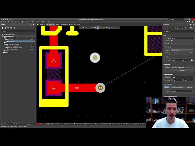
Tutorial 3 for Altium Beginners: PCB Layout
Комментарии:

Why do I always see 'random' numbers used for the Mechanical Layers?
They are never in perfect sequence like 1, 2, 3, 4, 5, etc. They are random like M2, M29, M16, etc?

I update Designator "D ?" in "D?", update, but no change in SchDoc...
Ответить
How to switch on display heads of information again
Ответить
Please tel l me cpwg impedance settings in altium
Ответить
Thank you for doing this wonderful and painstaking job. You are providing a chance to learn the Altium for a lot of students like me, I really appreciate it, sir
Ответить
work on your accent please.
Ответить
I'm having some issues about ımporting schematic to pcb phase. first I can't open project options because it's greyed out. second problem is I don't get "update pcb document" options in design segment. I have done everything right, I can't reach the pcb phase because of these two issues. can anyone help me please?
Ответить
This is a great video tutorial. I like the way you explain. I'm learning how to make footprints and 3D models for metal film or carbon film through-hole resistors that have color codes on their bodies. Tried searching but haven't found anything suitable. Anyone can help?
Ответить
How can I make only copper plate on PCB in Altium?
Ответить
The "left click"s annoyed me a bit lol
Ответить
Robert. I am trying to learn altium. I have a created pcb design. It is a big design. I am trying to find u1. I do not know what to type to find it. Please advice
Ответить
Hello, thank you for these helpful tutorials. Do you have any videos which show how to import an SMA connector 3D model and align in footprint?
Ответить
Where is the board outline?
Ответить
Big Thanks Sir, your Tutorial is very informative
Ответить
Thanks a lot for your video, it helped me to grab the main basics of using Altium. Thanks again
Ответить
Thanks
Ответить
good morning robert i have an error. I just follow your step my polygon can't connect to my via the polygon is gnd i dont why my via and polygon not connecting
Ответить
Hi Robert,
Thx for the tutorial, Super helpfull!
I've designed my diode footprint using the diode model instead of the resistor one as you did in this tutorial and I now it results in no rats being connected to either R nor Connector.
Any idea?
BR

Excellent tutorial! I've started to design my first PCB and this covers all the basics on how to drive Altium
Ответить
Hii sir,,, lots of love & respect. I am atif from india , i am very thankful to u & i dont have words to explain . i have never ever seen a teacher like u its feel like u r teaching us offline .
Ответить
this is a great video, thank you
Ответить
Simply awesome
Ответить
Great tutorial! The way to switch layers and automatically lace vias is now to hold shift and control and scroll while the place wire command is active. Pressing minus zooms out and pressing plus doesn't do anything
Ответить
Thanks for helping !!
Ответить
Super helpful, thank you!
Ответить
THANKS
Ответить
Hello Robert, how I can to change the schematic background color from white to black in altium?
Thanks!

Is there a way to disable the Generate Room option by default for a project? I would like it to be disabled for my template project so I don't always have to turn it off manually.
Ответить
I am only getting 4 options on the design option, what to do?
Ответить
hi Robert. How to define a distance between two pin headers to place esp nodemcu?
Ответить
Used Protel back in the late 90s, been using Eagle ever since, this series really helps figure out how to find all the new features that have been added and get started.
Ответить
THIS IS THE MOMENT OF THE TRUTH
Ответить
what is the difference between interactive route (ctrl+w) and place line ?
Ответить
Hello Robert,
When I create a document then I cannot see the project option,it shows in hidden mode.Can you please help me to find the solution of this problem?

Your tutorials are amazing! Very good examples, explenations an pace. Thank you!
Ответить
Tarraa french taraaaa
Ответить
Hi Robert,
Have you started using the latest Altium 20? I was following your tutorial but with Altium 20 instead of 18 - minor differences but I came across errors when doing the layer stackup (there are duplicates for whatever reason, the "work around" is changing the name of them I think. Was wondering if you saw similar issues or not.

Thank you so much !
Ответить
Hi,Rovert,I use AD14,when I import netlist into pcb,the .designator string I created in the mech layer is still .designator in th pcb,it did not auto change,why?
Ответить
Robert you are great !!!
Ответить
Nice video thanku ...one doubt is,can we generate board outline from design/ board shape/ create primitive from board shape/ then select the mechaniacal layer for out line. Is threre.any issues
Ответить
excellent tutorial 👍
Ответить
Excellent instruction Robert!!! Following, Watching and buying T Shirt!!! Thanks for the help in such a complete foundational way... a great start to build on.
Ответить
Hi, Robert! I wanted to ask that when i am going into the PCB format from the schematic, by update PCB document, in some of the pins it is showing "unknown pin error". Can you please tell me something about this error, i tried to correct it but, it's not working.
Ответить


