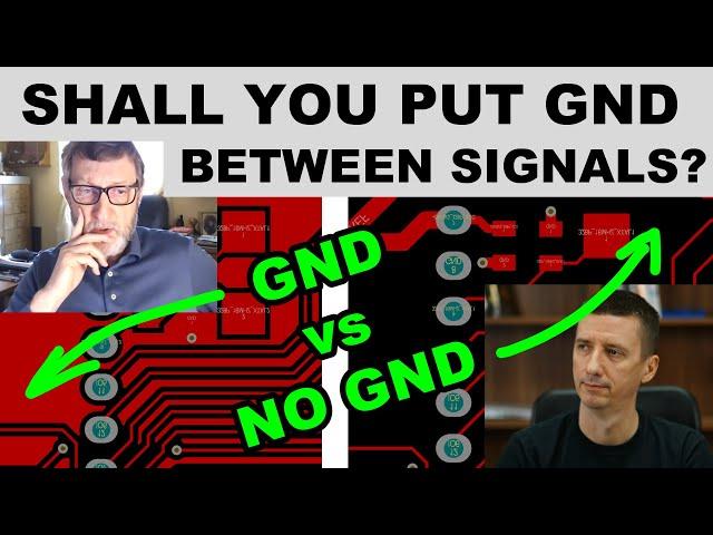
How to Decide on Your PCB Layer Ordering, Pouring and Stackup (with Rick Hartley)
Комментарии:

The most informative video on PCB design I have ever come across. You asked the right questions, and the guest was very experienced and prepared.
This one should be included in the curriculum for any aspiring PCB Design Engineers.
Thank you for the great work.

This is PCB design gold. Saving this to reference over and over again. Lots of great information and it's delivered in a way that is easier to understand than digging through all my books. Thanks for this!
Ответить
this explanasions were fantastic. I had lot of question about why the ground vias are required next to the some signal and all are answered. I appreciate your time for creating this video to share with others
Ответить
And that's why I like my 4 layer boards with ICs that have at least 5ns rise time. Anyway, thak you for very helpful video, I was always under the impresion that adding ground is pretty much always better, this makes much more sense.
Ответить
Awesome information. Congratulations.
Ответить
Uhhhhh great concepts!
But if I had told my boss that it was needed to go to a 6 layers board to iron out an emi problem ( and trust me, in the automotive world there's a lot of emi testing... Including the much feared " Bulk Current Test" , which is not an emi test whatsoever) I 'd have got fired in a microsecond!!
At that time ( ten years ago) the 32 bit microcontroller was already operating at 200 Mhz, so there was a lot of stuff to care about... and meeting the emi requirements was achieved without transitioning to a 6 layers board, that would have increasd the cost far beyond limits..
Instead a different solution was found , which was not 6 layers, and it worked fine! .
Maybe this guy just talks about the stuff he like most....

Very informative and great video, thank you very much dear Robert and Rick ❤🌺
Please post more videos of engineers' work experiences and how to solve challenges.

Hey Robert, great video and great guest! I have a question on the 12 layers board stack up. What if a signal has to pass from layer 1 to 4? There's a power plane in the middle, doesn't this generate a signal integrity problem for high frequency signals?
Ответить
this is great!
Ответить
Amazing!
Ответить
Thanks.
For the 12 layers stackup starting with Sig/Pwr, how do you manage shielding vias around single and differential tracks on top and bottom layers?

If traces are close to each other and carry high-frequency signals, this can lead to capacitive or inductive coupling effects, which can cause undesirable behavior in the system. Sometimes, to minimize these effects, a technique called "guard trace" or "ground guard" is used, which involves placing ground (GND) traces between critical signal traces. This technique can help reduce capacitive and inductive couplings.
However, if we're talking about resonance, it's a phenomenon that usually occurs when the length of the trace corresponds to a quarter of the wavelength of the signal carried by that trace. In such a case, standing waves can occur, which can cause signal quality problems. But for digital systems, such as microcontrollers, this is usually not a major issue because the lengths of the traces are much shorter than the wavelengths of the digital signals they carry.
In the general case, for systems based on microcontrollers such as the ATmega2560 (on which the Arduino Mega 2560 is based), the principle of using guard traces or additional GND traces is not necessary. These microcontrollers are usually used in low-frequency applications (up to tens of MHz), where effects such as capacitive or inductive coupling between closely spaced traces are less significant.

Thank you Robert. Your talks with experts like Rick Hartley and Eric Bogatin are videos that I visit every few months. Very grateful...
Ответить
Thank you very much for the great video!
In the customer problem described starting from minute 35, the solution is given by pouring copper on 4 layers and connecting them either to VCC or ground. However, it was also mentioned that the customer did not agree to change the layer stack and add more layers.
My questions are:
1. If adding layers is an option, would that be a better one rather than pouring?
2. Is there any disadvantage in adding another 2 or maybe even 4 layers having signal and ground separated, except the cost?

On resonances in cavities and ground stitching vias.
An analogy came to mind. It's like if you had a container with water. By swinging it back and forth with some frequency, you could easily achieve huge water oscillations.
But. If you divided that container by partitions into many small containers, you wouldn't be able to achieve that huge water oscillations at that frequency.
This is how ground stitching vias, by partitioning big cavities into smaller ones, prevent resonances in PCBs.
Thank you, Robert, for your videos! They are extremely useful.

could you please provide the slids? Thanks.
Ответить
You should make a clips channel or post more clips of interesting things said during interviews/videos. Would be pretty informative and worth wild
Ответить
this Q&A style is very helpful, I only understood it the second time Rick has explained if after your questions
Ответить
Are there any smaller versions of your videos with sort of conclusions/summary of dos and don'ts? While I am all for watching long videos, but sometimes shorter videos helps a lot.
Ответить
Excellent video. Very informative
Ответить
Have anyone tried the stack up order as Rick recommended like below?
- Signal/Power -
- Ground -
- Signal/Power -
- Ground -
Because I used to use stack up like this
- Signal/Ground -
- Ground -
- Power -
- Signal/Ground -
I would like to know which one has better EMI performance :)

I am still new to this world of electronics, I have never made even a 4 layer pcb, but I love seen your videos and learning new things. I would like to ask, how do you know so much about routing, materials, stackups, etc, and what would be the best way to get a better understanding of practical design considerations? Thank you very much for all the hard work!
Ответить
This is liquid gold. Thanks
Ответить
PLEASE stop ending videos in the middle of a conversation...........
Ответить
I didn't know that some parts can actually act as an antenna!
Ответить
Interestingly, Rick appears to disagree with Eric Bogatin regarding power or ground pours on signal layers. I'd like to hear them debate it with each other! I could be misunderstanding though. I'd also love to see the actual layer images for some of the stackups. It's hard for me to picture the Sig\power layers and how to would all be tied together.
Ответить
Hungarian accent
Ответить
PCB Design is no joke... I design for the military and I still get shocked by stuff like these
Ответить
Thank you so much
Ответить
Always excellent topics and videos, thanks for sharing such a great knowledge.
Ответить
Amazing, thank you.
Ответить
Oh man. Can I have a 3 min TL;DR? :D
Ответить
This is great video, thanks you so much <3 i had learn very much from your Channel !
Ответить
Thanks Robert, I fell I am watching 'God Father' movie for the first time 😁
Ответить
What about warpage when you don't have a symmetrical stack up? This was discussed in one of the other videos, so why don't you ask such questions when you have two different opinions? It would be helpfull, if you could ask experts such questions. I still don't get how you can have a ground plane on top and bottom. I think it is meant to be Signal/Ground and not only GND plane.
Ответить
I came back to this video to double check how to handle a 4 layer stack up, nice material, thanks !
Ответить
Do you need to do the full wavelength every 10th wavelength, or just the first Quarter wavelength every 10th wavelength?
Ответить
Intersting look on very importan topic.
Ответить
Federal. Such a great info packed interview w Rick. As usual. Took many notes. Please keep it up. I learn and relearn so much. Super fan, Todd.
Ответить
Thanks!
Ответить
problem goes away with optical traces.
Ответить
Great video!
Ответить
Great lessons in how stackup affects board performance. Thanks
Ответить
They should teach this kind of stuff on the university. That's a thousand times more useful than most other things.
Ответить
For hobbiest.. 6 layer is out of our league, 4 layers is our maximum. The price different between 4 layers to 6 layers is 9x 😭😭
Ответить
400gbit?? I wonder what the hell that things was....
Ответить
What does Dr Howard Johnson have to say about this?
Ответить
They are call it power planes meaning Power and Ground. The other Ground planes called Signal Ground planes
Ответить
Hi I have learnt so much from your tutorials can you guide from where can I get projects if I have to design new boards or the existing modified ones also any tutorials on routing bga packages
Ответить



![Gothic 2 - Returning Home 1 Hour [Extended] Gothic 2 - Returning Home 1 Hour [Extended]](https://invideo.cc/img/upload/UU9xSXVYX0RKVDc.jpg)


