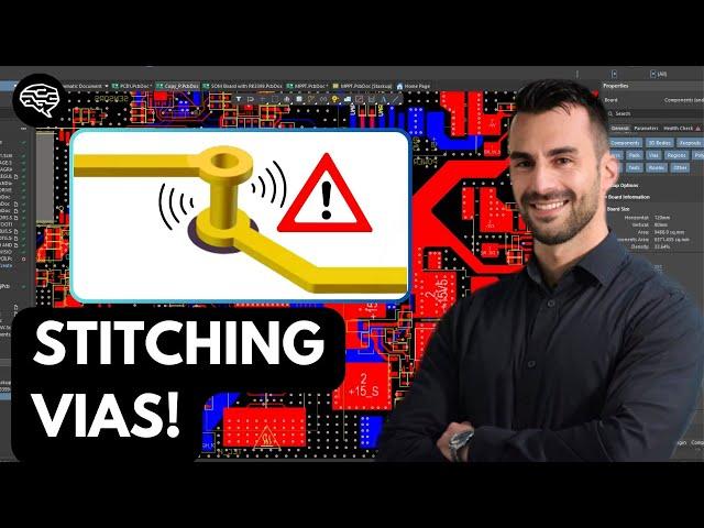
Stitching Vias PCB Simulation - PCB Layout for EMC and Signal Integrity
Become an EMI Specialist here: https://fresuelectronics.com
Free Courses: https://fresuelectronics.com/courses
----
If you don't know who I am:
I am an electronic engineer and IPC-certified designer with experience working for both small and large companies, as well as a top university worldwide.
Coming from a family that has been involved in the electrical and electronic field for four generations, I’ve been exposed to this industry since childhood, and my passion for it developed long before it became my profession.
I’m the owner and founder of fresuelectronics.com, where I provide PCB Design for Low EMI consultations, as well as marketing and design services related to PCB and EMC design.
My focus is on achieving first-pass success for EMI and EMC, as well as embedded digital design.
With my practical approach, I ensure that designs are both efficient and compliant with industry standards.
In addition to my consulting work, I run PCB Design Academies, where I share my expertise and passion with thousands of engineers and students.
Through my programs, I offer comprehensive training that covers the latest techniques and best practices in PCB design for low EMI, empowering engineers to create innovative and reliable products.
----
You can find my programs, academies, courses, and blog here: https://fresuelectronics.com
Dario If you want to become an EMI Specialist click here: https://fresuelectronics.com
----
If you don't know who I am:
I am an electronic engineer and IPC-certified designer with experience working for both small and large companies, as well as a top university worldwide.
Coming from a family that has been involved in the electrical and electronic field for four generations, I’ve been exposed to this industry since childhood, and my passion for it developed long before it became my profession.
I’m the owner and founder of fresuelectronics.com, where I provide PCB Design for Low EMI consultations, as well as marketing and design services related to PCB and EMC design.
My focus is on achieving first-pass success for EMI and EMC, as well as embedded digital design.
With my practical approach, I ensure that designs are both efficient and compliant with industry standards.
In addition to my consulting work, I run PCB Design Academies, where I share my expertise and passion with thousands of engineers and students.
Through my programs, I offer comprehensive training that covers the latest techniques and best practices in PCB design for low EMI, empowering engineers to create innovative and reliable products.
----
You can find my programs, academies, courses, and blog here: https://fresuelectronics.com
Dario
Тэги:
#PCB_Design #Circuit_Design #Electronic_Circuits #Printed_Circuit_Board #Schematics #Layout_Design #Signal_Integrity #PCB_Tutorial #Electronics_for_Beginners #PCB_Layer_Stack #EMI_in_PCB #Electronic_Engineering #PCB_Manufacturing #PCB_Assembly #Circuit_Board_Design #Professional_Electronics #PCB_Signal_Layers #Ground_Planes #PCB_Software #Component_Placement #PCB_Design_Guide #Electromagnetic_Compatibility #EMI #EMC #PCB #Altium #Kicad #Electronics #Maxwell_equationsКомментарии:

@yacineyaker7485 - 20.04.2024 17:04
great demonstration
Ответить
@naberx2 - 21.04.2024 12:13
I find this video very informative. Thank you for sharing.
Ответить
@Edwinthebreadwin - 23.04.2024 09:39
It’s rare to see electronic design advice like this, thanks for spreading the word
Ответить
@MarkVolosov-zb3wc - 03.05.2024 17:30
Love your videos keep up the good work!
Ответить
Как правильно нырять?
Школа подводной охоты Максима Лубягина
CAN YOU USE other brand wheels on the Thrustmaster T818?
Sim Racing Corner
Quarter Life - Virtual Bodies
onlyyesterday1967
Go Getter 1 Unit 5.2 I can fix it Part 1
Lavender's English
What Andrew Jordan did next | Inside Jordan Racing Team | Goodwood Masters
Goodwood Road & Racing


