How to Design PCB Layout using Eagle (CadSoft)
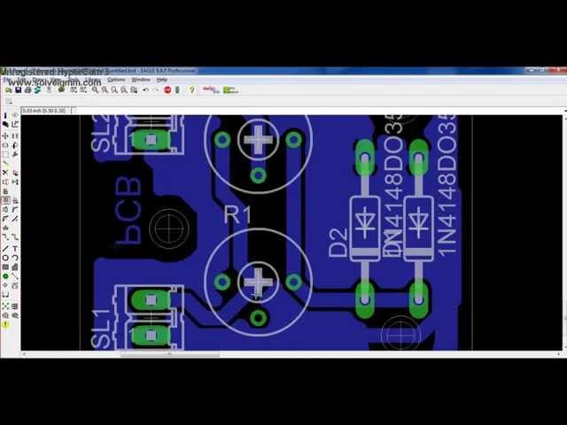
How to Design Schematic Diagrams and PCB Layout using Eagle from Cadsoft. This is a quick overview on how to design Schematic Diagrams and Printed Circuit Board (PCB) design Using Eagle.
My channel is all about electronics, laser engraving, engineering, repair do it yourself videos:
https://www.youtube.com/channel/UC-dVTz6la6JvXm1as7lL5Ng
If you want to learn more about electronics and Do it yourself, please subscribe to my channel:
https://www.youtube.com/channel/UC-dVTz6la6JvXm1as7lL5Ng?sub_confirmation=1
If you like this video, please watch my other electronics videos here:
https://youtube.com/playlist?list=PLT8ili7hfTtGWKrp_BWHeAisF7C1NYJXs
I release videos every 2nd and 4th week of the month. Please subscribe to see more
1.) Open Eagle: File; new; Schematic
2.) Add components using "Add" function
3.) Connect schematic symbols properly
4.) Switch to PCB layout view
5.) Resize PCB to desired dimensions
6.) place parts strategically: minimize complications on copper trace/routing from pins of one component to another
7.) Use "ratsnest" to calculate the shortest possible routes from one component to another. The yellow line serves as a guide to where the connection shall be made.
8.) use "route" and "unroute" to layout the copper traces of the components.
9.) use "Polygon" tool and set it to solid with spacing and isolation set, and then trace the entire PCB
10.) use "name" function and rename the polygon to GND (or name of your circuit ground)
11.) Use Ratsnest to apply the copper surface (to minimize the copper that's gonna be etched)
12.) Print it, (having the views only to the layers you want to print, specifically copper, pads, and dimensions).
Altium 365 trial link: https://www.altium.com/yt/KurtBarcelona
Octopart website: https://octopart.com/
by Kurt Barcelona, 2015.
Background Music: Jahzzar - Missing You. I do not own the music. Fair use.
Тэги:
#how_to_design_pcb #how_to_make_pcb #how_to_use_eagle #how_to_design_using_eagle #pcb_layout #eagle_soft #cadsoft #how_to_design_schematic_diagrams_using_eagle #eagle #printed_circuit_board_design #designing_pcb #Electronics_(Field_Of_Study) #PCB_designКомментарии:
How to Design PCB Layout using Eagle (CadSoft)
Kurt Barcelona
Wild card entry to BDC Round 4 2022
SMT MOTORSPORT
Duet maut ratu tiktok(2)
Delon Adenaputra
La alianza reacciona al simp es gojo satoru vs sukuna [parte 2]
Elite brown cameraman
В Волгограде обсудили развитие городского электротранспорта
Муниципальное телевидение Волгограда


![FREE TWITCH FOLLOW BOT [2021] (+34 FREE TOKENS) FREE TWITCH FOLLOW BOT [2021] (+34 FREE TOKENS)](https://invideo.cc/img/upload/QTJreVUzWlh1T3k.jpg)


![La alianza reacciona al simp es gojo satoru vs sukuna [parte 2] La alianza reacciona al simp es gojo satoru vs sukuna [parte 2]](https://invideo.cc/img/upload/c05WLTJ4MU00NmQ.jpg)


